- Undergraduate
Bachelor's Degrees
Bachelor of ArtsBachelor of EngineeringPartner School Dual-DegreeUndergraduate AdmissionsUndergraduate Experience
Quick Links
- Graduate
Doctoral Degrees
Doctor of PhilosophyPhD Innovation ProgramDoctor of Medicine-PhDGraduate AdmissionsGraduate Experience
Quick Links
- Research
Research by Program Area
Quick Links
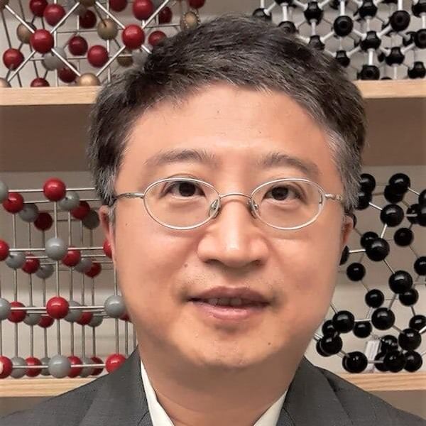
Jifeng Liu
Professor of Engineering
Program Area Lead: Materials Science & Engineering
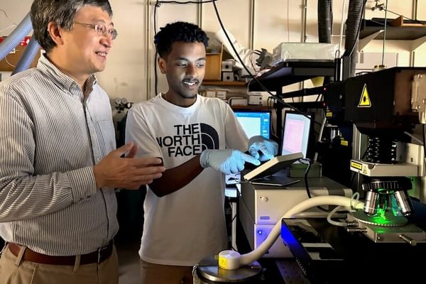
Professor Liu and PhD candidate Gideon Kassa conducted experimental follow-up testing to confirm the properties and potential of a newly discovered photovoltaic material. (Photo by Catha Mayor)
Research Interests
Optoelectronic materials and devices; integrated nanophotonics for energy-efficient Information Technologies (Green IT); Nanomaterials and nanostructures for solar cells and thermophotovoltaic cells; Infrared and ultraviolet optical sensors
Education
- BS/MS, Materials Science and Engineering, Tsinghua University, China 2001
- PhD, Materials Science and Engineering, Massachusetts Institute of Technology 2006
Awards
- Fellow, The Optical Society, 2021
- NSF CAREER Award, 2012
- Materials Research Society (MRS) Graduate Student Gold Award, 2004 MRS Fall Meeting
Professional Activities
- Co-chair, sub-committee of Electronic-Photonic Synergy on Si, 2013 IEEE International Conference on Group IV Photonics
- Review Editor and Topical Editor in Silicon Photonics, Frontiers in Materials
- Organization Committee, The Electrochemical Society (ECS) SiGe, Ge and Related Compounds Symposium
- Session Chair in silicon photonics and solar materials at ECS, IEEE Photonics Society and OSA conferences
- Vice Chair, Photonic Devices and Optoelectronic Integration Sub-Committee, 2012 (43rd) International Conference on Solid State Device and Materials
- Technical Program Committee Member, 2012 International SiGe Technology and Device Meeting
Research Projects
-
High-strength, high-ductility, high entropy alloys with high-efficiency native oxide solar absorbers for concentrated solar power systems
High-strength, high-ductility, high entropy alloys with high-efficiency native oxide solar absorbers for concentrated solar power systems
This project is investigating the synergy between the excellent mechanical behavior of FeMnNiAlCr high entropy alloys (HEAs) and the high solar absorptance of their native thermal oxides for high efficiency concentrated solar thermal power (CSP) systems working at >700oC. The alloy itself would be used in high-temperature tubing to carry molten salts or supercritical carbon dioxide (sCO2), while the native oxide would act as a high-efficiency solar thermal absorber. The oxide layer is also dense and protective against oxidation (parabolic growth kinetics) at 750 °C. This new Fe-Mn based HEA system has already demonstrated a higher tensile strength and ductility than more expensive Ni-based Inconel 740 superalloys at both room temperature (with carbon doping) and 750oC (with Ti doping), and their native thermal oxides have achieved a high optical-to-thermal conversion efficiency of ηtherm=90.8% at 750°C under 1000x solar concentration ratio. In preliminary corrosion studies, two-phase Cr-modified HEAs have sustained bromide molten salts for 14 days at 750°C with <2% weight loss. The project has close collaborations with the Oak Ridge National Laboratory (ORNL) and the Ames Laboratory in computational materials science and atom probe tomography (APT) to understand the fundamental structure-property relationship in FeMnNiAlCr HEAs.
Funded by DOE.
-
Integrated nanophotonics devices for high-bandwidth, ultra-low energy photonic data links
Integrated nanophotonics devices for high-bandwidth, ultra-low energy photonic data links
Integrated nanophotonics devices for high-bandwidth, ultra-low energy photonic data links offer solutions to the increase in energy consumption from computation and communication systems that has come with the rapid growth of information technology in the 21st century. Data transmission starts to consume even more energy than data processing in microprocessors, servers and data centers due to resistive losses and RC delay in electrical interconnects. Optical interconnection, on the other hand, does not have bandwidth limit or resistive losses as its electrical counterpart, thereby providing an idea solution to high bandwidth, ultralow energy data links. Our research aims to integrate nanophotonic devices monolithically on silicon chips to achieve electronic-photonic synergy, combining the merits of photons in data transmission with electrons in data processing. Recent research focuses on low-temperature (<450C) integration of nanophotonic devices such as photodetectors and photonic modulators with back end of line (BEOL) CMOS technology.
-
Self-assembled nanophotonic structures for light trapping in solar cells
Self-assembled nanophotonic structures for light trapping in solar cells
Self-assembled nanophotonic structures for light trapping in solar cells can help with the critical task of reducing $/W for large scale applications. In conventional wafer-based solar cells, material alone constitutes more than half of the cost. Thin-film solar cells have become an attractive solution in recent years due to a drastic decrease in material consumption by 100x. The trade-off, however, is that their efficiency is limited by the thickness of the cells which is insufficient to absorb all the sunlight. Light trapping is needed to increase the optical path length of sunlight in these thin-film solar cells in order to improve the efficiency. In this research we are investigating self-assembled nanophotonic structures integrated on the backside of thin-film solar cells for sunlight trapping. The nanophotonic structure diffracts the incident sunlight into oblique angles so that it propagates laterally in the thin films and gets completely absorbed. Recent work demonstrated nanophotonic structures using self-assembled porous anodic aluminum oxide as a fabrication template for effective light trapping.
-
Band-engineered semiconductors and phosphor materials for efficient solid-state lighting
Band-engineered semiconductors and phosphor materials for efficient solid-state lighting
Band-engineered semiconductors and phosphor materials for efficient solid-state lighting contributes toward the development of sustainable lighting technology for the 21st century. Lighting consumes ~1 TW of power worldwide, with greenhouse gas emission equivalent to 70% of the world's car emission. Solid-state lighting using semiconductor light emitting diodes (LEDs) has been widely recognized as the next generation energy-efficient lighting technology, since LEDs feature superior efficiency, longer lifetime, and lower environmental hazard when compared with conventional lighting sources. Currently a blue LED is usually combined with phosphor coating to generate white light. There are two major challenges to this technology: (1) LED Efficiency droop at high current density required for lighting; (2) Optical energy losses due to converting blue photons to lower energy photons by phosphors. To attack the former issue we are exploring band-engineering of semiconductors near direct-indirect gap transition to achieve anti-droop properties. For the latter issue we are investigating more efficient phosphor materials especially in the yellow-red regime to enhance its conversion efficiency. We are also conducting research on long-afterglow phosphors which can store optical energy during the day and emit light at night for emergency lighting and decorative lighting.
-
Visible-blind and solar-blind ultraviolet detectors for flame and oil spill detection
Visible-blind and solar-blind ultraviolet detectors for flame and oil spill detection
Visible-blind and solar-blind ultraviolet detectors for flame and oil spill detection are useful for solving the technical challenge of operating these detectors with a large background radiation of sunlight. UV detection in the wavelength range of 210-300 nm is useful for flame, oil spill and missile detection, and traditional approaches include wide band gap semiconductor UV photodetectors and vacuum-based photoemission detectors. We are investigating more effective and less costly technologies for UV detection, including self-assembled visible light filters and solid-state photoemission detectors based on metal nanoparticles with plasmonic enhanced responsivity.
-
Environmental-benign Group IV (Si, Ge, Sn) nanomaterials
Environmental-benign Group IV (Si, Ge, Sn) nanomaterials
Environmental-benign Group IV (Si, Ge, Sn) nanomaterials for solar cells, thermophotovoltaic (TPV) cells, and infrared photodetectors are being used to address the issue of sustainability as, in the case of solar cells, it is highly desirable to use naturally abundant, environmentally-friendly materials. Currently Si, CdTe and CuInGaSe2 (CIGS) are dominating solar cell materials. Although thin-film CdTe and CIGS solar cells offer higher efficiency their Si rivals, the rarity of Cd, In, and Se elements makes it impossible for them to meet a meaningful portion of global energy needs. The toxicity of Cd also raises environmental concern. By comparison, Group IV materials (Si,Ge,Sn) are very attractive due to their high abundance and low toxicity. Furthermore, (Si,Ge,Sn) alloys and nanostructures have already demonstrated many interesting properties surpassing Si, such as wide range of band gap tenability and direct gap behavior. These properties can potentially lead to better performance than CdTe and CIGS cells. We are investigating material growth, defect passivation, and band-engineering of these environmental-benign Group IV nanomaterials for solar cells and thermophotovoltaic (TPV) cells (direct conversion of thermal radiation to electricity). Similarly, in mid and far infrared photodetectors the dominant HgCdTe material may also be substituted by environmental benign, cost-effective GeSn or Sn nanostructures to achieve IR sensing and night vision.
-
High-temperature solar absorbers for solar thermal systems
High-temperature solar absorbers for solar thermal systems
High-temperature solar absorbers for solar thermal systems are complementary to solar cells as another way of harvesting solar energy. The energy conversion efficiency increases with the working temperature of solar thermal systems according to the second law of thermodynamics. A critical component to achieve high working temperature is solar absorber coatings, which should absorb sunlight and convert it to heat efficiently with minimal thermal radiation loss in the infrared regime. They should also be stable at high temperatures. In this research we are investigating optical absorbers based on oxidation-resistant cermet materials incorporating metallic nanoparticles in a ceramic matrix for a working temperature of >560 C. Instead of using metal nanoparticles which are either easily oxidized at this temperature or too expensive to apply in large quantities, we are exploring certain metallic compounds that combines metal-like optical absorption properties with ceramic-like chemical stability. We also engineer the microstructure of the coating to trap infrared thermal radiation within the solar absorber coating and further increase the working temperature.
-
Rare-earth selective emitters for high efficiency TPV systems
Rare-earth selective emitters for high efficiency TPV systems
Rare-earth selective emitters for high efficiency TPV systems address the major limiting factor for the efficiency of TPV cells: the broad emission spectrum from the heat source. Photons with energy smaller than the band gap of semiconductor PV materials cannot be absorbed, while for those with energy much greater than the band gap the excess energy is lost to heat instead of generating electricity. Although there is nothing we can do to change the solar spectrum, for thermal sources of TPV systems we may engineer the thermal emission spectrum by using certain coatings called "selective emitters." Using this approach, the broad blackbody emission spectrum can be condensed to a much narrower band that optimally matches the absorption spectrum of semiconductor TPV cells. In particular, we are investigating rare-earth ceramic selective emitters such as Yb and Er compounds to match the absorption of Si and Ge TPV cells. We are also engineering the microstructures of these compounds to manipulate photons for enhanced selective emitting performance.
-
Porous thermoelectric cells (TECs) for waste heat recovery
Porous thermoelectric cells (TECs) for waste heat recovery
Porous thermoelectric cells (TECs) are being developed for waste heat recovery. This project seeks to convert waste thermal energy directly into electricity potentially increasing overall energy efficiency by 15-20% and providing new portable electric power sources, particularly for cold regions. The project is focusing on low cost, nanostructure-engineered TEC (NETECs) materials based on earth-abundant, highly machinable metallic alloys and intermetallic compounds by engineering the grain sizes, second phase precipitation, and nanopores in transition metal intermetallic compounds. The project is currently focusing on the compound Fe2AlV. The location of quaternary atoms in the lattice is being determined by the TEM-based technique ALCHEMI.
Funded by USA-CRREL
Selected Publications
- Xiaobai Yu, Xiaoxin Wang, Qinglin Zhang, Juchuan Li, and Jifeng Liu, “Oxidation-resistant, solution-processed plasmonic Ni nanochain-SiOx (x < 2) selective solar thermal absorbers,” Journal of Applied Physics 116, 073508 (2014)
- Jifeng Liu, “Monolithically Integrated Ge-on-Si Active Photonics,” Photonics 1, 162-197 (2014) (Invited Paper)
- Haofeng Li, Jeremy Brouillet, Alan Salas, Xiaoxin Wang, and Jifeng Liu, “Low temperature growth of high crystallinity GeSn on amorphous layers for advanced optoelectronics,” Optical Materials Express 3, 1385–1396 (2013)
- X.X. Wang, L.C. Kimerling, J. Michel, and J.F. Liu “Large inherent optical gain from the direct gap transition of Ge thin films,” Applied Physics Letters 102, 131116 (2013)
- X.X. Wang, H. Li, Y. Cai, R. Camacho-Aguilera, L.C. Kimerling, J. Michel, and J.F. Liu, “Infrared absorption of n-type tensile-strained Ge-on-Si,” Optics Letters 38, 652 (2013)
- X.X. Wang, H. Li, X. Yu, X. Shi, and J.F. Liu, “High-performance solution-processed plasmonic Ni nanochain-Al2O3 selective solar thermal absorbers,” Applied Physics Letters 101, 203109 (2012)
- J.F. Liu, L. C. Kimerling, and J. Michel, “Monolithic Ge-on-Si lasers for large-scale electronic-photonic integration,” Semiconductor Science and Technology 27, 094006 (2012) (Editor’s Choice for 2012 Highlights Collection)
- J.F. Liu, R. Camacho-Aguilera, J.T. Bessette, X. Sun, X.X. Wang, Y. Cai, L.C. Kimerling and J. Michel, “Ge-on-Si Optoelectronics,” Thin Solid Films 520, 3354 (2012)
- J. Michel, J.F. Liu, and L.C. Kimerling. "High performance Ge-on-Si photodetectors," Nature Photonics 4, 527 (2010)
- J.F. Liu, X.C. Sun, L.C. Kimerling and J. Michel, "A Ge-on-Si laser operating at room temperature”, Optics Letters 35, 679 (2010)
Patents
- UV/VIS/IR back-side-illuminated photon-counting sensor | 11,522,098
- Nanophotonic hot-electron devices for infrared light detection | 11,462,656
- Method and apparatus of surface-incident, plasmon-enhanced multiple quantum well modulators and optical coupling thereon | 10,656,443
- Method of forming single-crystal semiconductor layers and photovoltaic cell thereon | 9,356,171
- Engineering emission wavelengths in laser and light emitting devices | 8,242,480
- High speed and low loss GeSi/Si electro-absorption light modulator and method of fabrication using selective growth | 8,160,404
- Ultrafast Ge/Si resonator-based modulators for optical data communications in silicon photonics | 7,840,099
- Method of fabricating Ge or SiGe/Si waveguide or photonic crystal structures by selective growth | 7,801,406
- Method and structure of germanium laser on silicon | 7,596,158
- Vertically-integrated waveguide photodetector apparatus and related coupling methods | 7,305,157
- Integrated waveguide photodetector apparatus with matching propagation constants and related coupling methods | 7,266,263
- Method of forming Ge photodetectors | 6,946,318
- Ge photodetectors | 6,812,495
Courses
Videos
Seminar: Nanophotonics for Sensing and Sustainability
Dartmouth PhD Innovation Program: Zhiyuan Wang
Graduate Student Engineering Research: Crystalline Germanium
News


In the News
pv magazine International
Scientists identify new ‘promising’ absorber material for thin-film solar cells
Mar 18, 2024
Scientists identify new ‘promising’ absorber material for thin-film solar cells
Mar 18, 2024
Global Solar Technology
Solar-Tectic LLC gets exclusive license for manufacturing single c-Si thin-films on ordinary glass
Feb 01, 2012
Solar-Tectic LLC gets exclusive license for manufacturing single c-Si thin-films on ordinary glass
Feb 01, 2012
Optics and Photonics News, Optical Society of America
The beginning of truly integrated lasers?
Apr 11, 2011
The beginning of truly integrated lasers?
Apr 11, 2011