
About
The Dartmouth Solid State Microengineering Laboratory includes class 100 and 1000 cleanroom laboratories, located in room 223 of Cummings Hall at the Dartmouth College Thayer School of Engineering.
Typical research includes applications in microelectronics, bio-integrated and biomedical devices, micro-electro-mechanical systems, quantum computing, sensors, energy, and photonics. Equipment is available for photolithography, e-beam lithography, wet chemical processing, plasma etch, film deposition and analysis.
The microengineering laboratory is available to qualified members of the Dartmouth community, and by arrangement to other local research interests.
Students with projects in the cleanroom range from first year undergraduates to graduate students. Classes that use the cleanroom include: Science of Materials (ENGS 24), Nanotechnology (ENGS 134), Thin Films and Microfabrication Technology (ENGS 135), Molecular Sensors & Nanodevices in Biomedical Engineering (ENGS 159).
News & Highlights
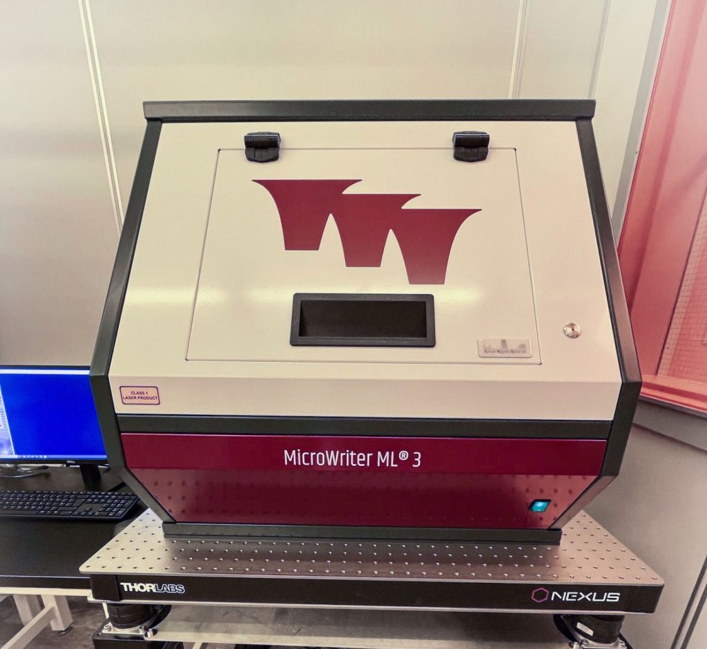
Maskless Aligner
A new maskless aligner was installed in November of 2023.
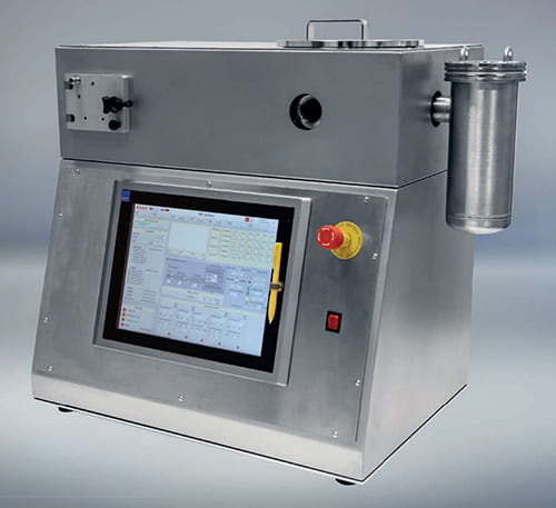
Parylene Coater
A new Parylene coater was installed in October of 2023.
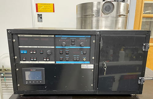
Reactive Ion Etcher
A rebuilt Reactive Ion Etcher was installed in March of 2023.